Quantum technologies
MENU
Technical Marketplace
»
Service providers
»
back
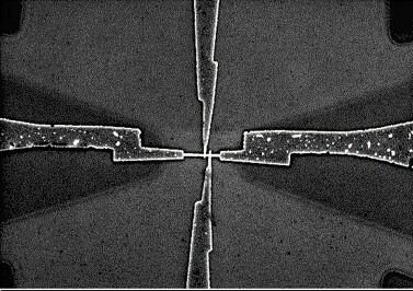
Example of high resolution lithography
Litho test structures for quantum manufacturing
Organization name
CSIC
Service
Qu-Pilot
Description
The lithography demands for the manufacturing of semiconductor quantum devices are quite stringent, sometimes beyond what it is available at the present. We offer the possibility to deliver test structures designed specifically to develop and/or validate new advances in lithography for qubit manufacturing, primarily aimed at process equipment companies. The pilot line for fabrication of semiconductor quantum devices can deliver test structures designed on purpose to characterize specific lithography methods, for example to improve overlay alignment or to characterize repeatability. Characterization facilities at the pilot line can be used to benchmark the results.
Service number
Interested in service?
Example of nanoelectrodes aligned on a pre-patterned substrates
Document 1
Lithography test structures for quantum manufacturing. Specifications
Document 2
Applications
Sensing
Computing
TRL
3
Platform
Semiconducting
Offering type
Prototyping
Testing
Fabrication
Link to Service providers
Similar products
CMOS compatible qubit electrodes
Qu-Pilot
Fraunhofer Institute for Photonic Microsystems IPMS
Contact test structures for quantum manufacturing
Qu-Pilot
CSIC
Diamond Lens Devices (SIL)
Qu-Pilot
TNO
E-mail
Contact person
Contact function
Organization name
You can write a note here.