Quantum technologies
MENU
Technical Marketplace
»
Service providers
»
back
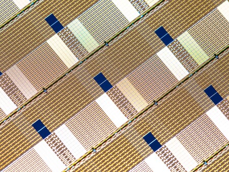
3-inch wafer with III-V SPADs
Fabrication of III-V APDs and SPADs
Organization name
Fraunhofer IAF
Service
Qu-Pilot
Description
The offered development services of III-V photonic components aim particularly for APDs and SPADs for the short-wave infrared spectral bands with detection wavelengths around 1550 nm. For this purpose, Fraunhofer IAF can draw on its long-standing III-V epitaxy and process technology for the InGaAs/InP-based material system. The fabricated detector devices can be I-V characterised on-wafer and electro-optically characterised on-chip in a dedicated lab setup. Epitaxial growth and process technology of III-V optoelectronic components, especially InGaAs/InP pin-PDs, APDs, and SPADs. Wafer diameters: 76.2 mm (3 inch), 100 mm (4 inch), multi-project wafer compatible
Service number
Interested in service?
SEM image of a single InGaAs/InP SPAD with 10-µm active diameter
Document 1
III-V SPAD devices and process test structures ready for on-wafer characterisation
Document 2
Applications
Sensing
Communication
TRL
4
Platform
Photonics
Offering type
Prototyping
Fabrication
Link to Service providers
Similar products
III-V photodetector characterisation
Qu-Test
Fraunhofer IAF
SWIR Single Photon Detectors
Qu-Pilot
Fraunhofer HHI
Telecom single-photon detector characterization
Qu-Test
Fraunhofer IAF
E-mail
Contact person
Contact function
Organization name
You can write a note here.