Quantum technologies
MENU
Technical Marketplace
»
Service providers
»
back
Diamond device with DC and MW gate-structures being wire-bonded in a PCB.
Diamond Lens Devices (SIL)
Organization name
TNO
Service
Qu-Pilot
Description
We have developed a stable process to procure diamond substrate (in 100 or 111 crystalline orientation), adjust the density of in-grown NV centers, manufacture micrometer-sized lenses around single NVs (sometimes referred to as SIL [solid-immersion lens]), add metallic gating structures (MW and DC), and anti-reflective coating. These devices can be delivered bonded in a PCB. Typically, the best lens can achieve about one million photons per second from a single NV (disregarding photons from other sources). Beyond this, some customer-supplied substrates and color centers can be used – please inquire with us to discuss details. Several of the micro-lens devices we made were used for the The Hague-Delft quantum internet demonstrator [https://arxiv.org/abs/2404.03723], among others. They have also been used to enhance the readout of diverse individual or ensemble color centers, significantly enhancing and accelerating (complex) measurements. This can e.g. be used to accelerate investigations of (novel) color center candidates, protocol development, QKD and quantum internet development, fundamental research, etc. If you have any more questions, inquiries, or custom requests, please do not hesitate to reach out.
Service number
Interested in service?
Scanning-electron micrograph image of a lens in diamond around a single NV with microwave and DC bias gates and anti-reflective coating.
Document 1
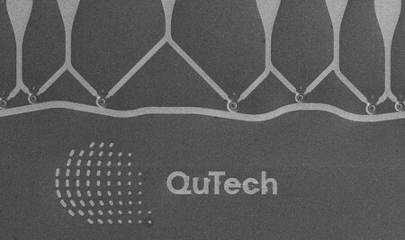
Scanning-electron micrograph image of multiple lenses, gates, and logo.
Document 2
Applications
Sensing
Computing
Communication
TRL
Platform
Diamond
Offering type
Prototyping
Testing
Measurements
Design support
Fabrication
Link to Service providers
Similar products
Confocal NV characterization
Qu-Pilot
TNO
FIB fabrication of Si and Ge color centers
Qu-Pilot
FBK
Characterization of Diamond-Based Qubits
Qu-Test
E-mail
Contact person
Contact function
Organization name
You can write a note here.