Quantum technologies
MENU
Technical Marketplace
»
Service providers
»
Filter
Sort
back
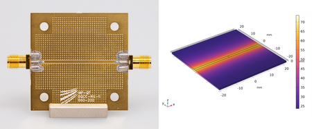
Antenna PCB Design - Example of manufactured antenna and heat simulation for efficient characterization and qubit driving
Design of RF PCB Antenna Boards
Organization name
Fraunhofer IAF
Service
Qu-Pilot
Description
We provide custom design, fabrication, and characterization of RF antenna PCBs for quantum technology applications, with a focus on NV-center-based systems in diamond. Our service covers the full development chain, from electromagnetic simulation and antenna design to PCB manufacturing and experimental validation. We specialize in coplanar waveguide (CPW) antenna structures optimized for efficient magnetic field generation at the quantum device location. A key feature is the development of dual-frequency antenna boards, enabling operation in both the RF (MHz) and microwave (GHz) regimes. This allows simultaneous control of nuclear and electron spins within a single integrated platform. The delivered PCBs are optimized for low losses, efficient power usage, and reliable integration into experimental setups. Optional services include RF characterization (S-parameters) and preparation or integration of diamond samples for immediate use in quantum experiments.
Service number
2
Interested in service?
Document 1
Document 2
Applications
Sensing
Computing
TRL
Platform
Diamond
Offering type
Prototyping
Testing
Link to Service providers
E-mail
Contact person
Contact function
Organization name
You can write a note here.